Behringer DCX2496 Project (DCX2496 mod; 改造)
There are several projects to modify DCX2496. Some are improving analog circuit or power supply quality, while others add 3 band (Low/Mid/High) digital (SPDIF) outputs.
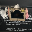
DCX2496 has a digital input as standard, so what I need is just to add 2 band digital outputs. I did not cut or replace existing components but just soldered 8 wires to the main board, except a RJ45 connector hole between AC input and RS-232C connector.
sorry for ugly finish
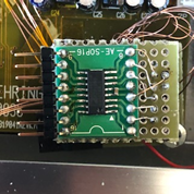
Soldering wires to the main board
I have connected 8 wires to the main board, 2 out of 8 wires are not used at this moment, but future use. Red arrow shows 1 thrugh 6, and 7&8 are on the other side of the circuit board.
- Low Freq. Data: R54 (IC4 side) or pin 6 of IC4
- Mid Freq. Data: R55 (IC5 side) or pin 6 of IC5
- High Freq. Data: R56 (optional, IC6 side) or pin 6 of IC6
- ACLK12: pin 3 of IC4* (optional)
- BCLK: pin5 of IC5*
- LRCLK: pin7 of IC6*
- GND: pin 2 of IC7 or IC9 (5V regulator) from bottom side of the board
- Power: pin 1 of IC7 or IC9 (5V regulator) from bottom side of the board
*can be connected to any of IC4, IC5, IC6
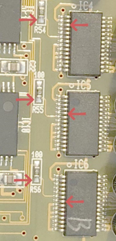
IC4, 5, 6 are AK4393 D/A converters with 28 pins, 0.65mm pitch. When connecting to IC4, 5, or 6, cover up adjacent pins with Kapton tape and solder a wire. Kapton tape is not necessarily removed and leave as is. The tape may reduce the chance to bridge solder to the next pin. I carefully soldered 2UEW 0.29mm wire. Soldering wires to R54, R55, R56 also needs attention because too much heat may move those registers.
Circuit
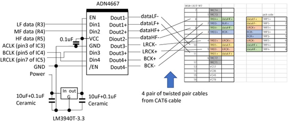
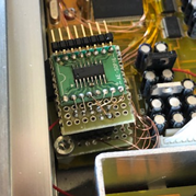
All wires are connected to a small daughter board with 3.3V regulator and a connector to grand-daughter board. Daughter board also has 5V regulator, and connection to HF data, as well as ACLK for future use, and attached to the housing via a screw through daughter-board - 10mm spacer – main-board. The grand-daughter board sits on the daughter borad's connector and has a LVDS driver (ADN4667) and a connector for output.
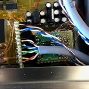
The output is LVDS level, via a 1000 Base-T RJ-45 (0838-1X1T-W7) connector. It has 4 isolation transformers built in and impedance is well controlled to 110ohm when used with CAT6 cable. Note that system clock (ACK from Pin3 of IC3, 4, or 5) is not connected to the output, because there is no vacant line, and Sample Rate Converter SRC4193 or SRC4192 does not require system clock from I2S source.
I have assigned High frequency to MF of DCX2496, so MF output is renamed to dataHF+/- at output side of ADN4667.
The connection of 1000baseT is based on Accuphase’s HS-LINK, where KEY is replaced with dataHF+/-.
(Optional)
Those who need 2 or 3 band SPDIF output, you can use one DIT4192 per band clocked with ACLK signal. DIT4192 ‘s TX+(pin 18)/TX-(pin17) can be wired to each pair of RJ-45 connector via a 0.1uF capacitor and a 110ohm register connected serially and use an RJ-45 connector with isolation transformers. At the other end of CAT6 cable, you may use another RJ-45 connector with transformer to connect XLR connectors (AES/EBU).
As of Feb 18 2021, modification is done, but have never been tested yet.
DCX2496の改造は、アナログ回路や電源を改善するものや、帯域ごとにSPDIF出力を追加するものがあるようです。
DCX2496は標準でデジタル入力が可能なので、2バンドのデジタル出力を追加することにしました。改造は、回路を切ったり部品を取り替えたりはせず、電線をはんだ付けすることと、RJ-45の穴を電源とRS-232Cコネクターに取り付けるだけにしました。
メインボードへの電線の取り付け
下記のように、8本の電線をメインボードにはんだ付けしました。8本中、2本は将来のためで、現状は使っていません。
- 低域データ: R54 (IC4側) または、IC4の6ピン
- 中域データ: R55 (IC5側) または、IC5の6ピン
- 高域 Data: R56 (予備, IC6側) または、IC6の6ピン
- ACLK12: pin 3 of IC4* (予備)
- BCLK: pin5 of IC5*
- LRCLK: pin7 of IC6*
- GND: pin 2 of IC7 or IC9 (5V レギュレータ) 基板の裏面に接続
- 電源: pin 1 of IC7 or IC9 (5V regulator) 基板の裏面に接続
* IC4, IC5, IC6の何れでも可
IC4, 5, 6 は AK4393 D/A コンバータで0.65mm間隔の28ピンです。電線を接続する際は、ハンダブリッジを予防するために、隣の両側のピンをカプトンテープで覆ってから、2UEW 0.29mmをはんだ付けしました。カプトンテープは貼ったままで大丈夫です。R54, R55, R56にハンダ付けする際、加熱しすぎると抵抗がずれてしまうので要注意です。
3.3Vのレギュレータとコネクタを載せたドーターボードに全ての電線を接続します。予備で5.0Vのレギュレータも搭載し、高域データとACLKも接続しています。ドーターボードは、スペーサーとメインボードを介して本体にネジ止めしました。孫ボードには、孫ボートはLVDSドライバADN4667と、出力コネクタを搭載しています。
高域の出力が必要な場合や、SPDIF出力が必要になったときなど、孫ボードを作り変えることができます。
出力はLVDS信号で、1000 Base-T RJ-45 (0838-1X1T-W7)コネクタに出力します。このこねくたには、アイソレーショントランスが搭載され、CAT6ケーブルを使えば、インピーダンスも正確に110Ωに合わせられます。なお、出力コネクタに空きがないため、システムクロック(ACK)は出力されません。サンプルレートコンバーターの SRC4193 or SRC4192 を使えば、I2Sの信号源にはクロックは必要無いためです。DCX2496は、中域に高音を設定しているので、中域の信号は、ADN4667の出力側以降はdataHF+/-としています。
1000BaseTの接続はアキュフェースのHS-LINKを参考に、KEYをdataHF+/-に差し替えています。
(おまけ)
2~3バンドのSPDIFが必要な向きには、バンドごとに、DIT4192を使うことができます。クロックはACLKからとり、DIT4192のTX+(pin 18)/TX-(pin17) を、0.1μFと110Ωをシリーズ接続してRJ-45 に接続できます。CAT6ケーブルの終端には、同様にトランス付きのRJ-45コネクター経由でXLR(AES/EBU)に接続することができます。
2021年2月18日現在、改造は済んでいますが、まだテストできていません。